










New Delhi: As India aggressively positions itself as the next global hub for electronics and semiconductor manufacturing, industry leaders are warning that the country’s current policy framework remains incomplete. While billions of dollars in subsidies and government backing have successfully attracted major global players to set up fabrication (fab) and packaging (OSAT) units on Indian soil, a critical missing link threatens to undermine long-term self-reliance: the domestic production of semiconductor equipment, subsystems, and specialized components.
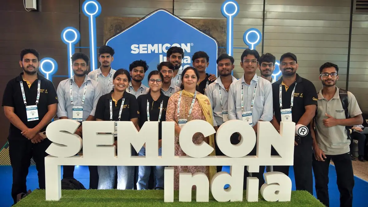
Speaking at the recently concluded Semicon India conference, a senior executive with the KAS Group of companies delivered a stark assessment of the nation’s technological roadmap. According to the executive, if India genuinely aspires to build a deep, resilient, and self-sustaining local manufacturing ecosystem, New Delhi must urgently introduce dedicated government incentives specifically tailored for developing semiconductor equipment within the country.
This sentiment reflects a growing consensus among engineering firms, supply chain experts, and multinational technology providers who argue that fab units alone cannot sustain a thriving semiconductor economy without an indigenous machinery and tools ecosystem to support them.
1. Main Facts: The Missing Link in India’s Semiconductor Strategy
The core argument emerging from industry voices at Semicon India is straightforward: building chips requires highly specialized, multi-million-dollar machinery—ranging from photolithography and etching tools to cutting, grinding, and polishing systems. Currently, India imports 100% of these foundational manufacturing tools.
- Beyond the Fab: While central and state governments have rolled out lucrative production-linked incentive (PLI) schemes and capital support for semiconductor fabrication plants and Outsourced Semiconductor Assembly and Test (OSAT) facilities, the machinery, components, and intellectual property (IP) running these plants remain entirely foreign.
- The KAS Group Proposal: A senior executive from the KAS Group emphasized that government support must dynamically expand beyond the wafer-fabrication plants to encompass the entire upstream technology and supply chain ecosystem.
- Focus on R&D and Prototyping: The executive called for specialized equipment Research and Development (R&D) incentives, arguing that financial backing is critically required to help domestic entities design, prototype, and commercialize high-tech semiconductor tools.
- Infrastructure Deficit: India currently suffers from a scarcity of pilot lines, reference facilities, and certified testbeds where domestic startups and established engineering firms can rigorously test their newly developed tools against strict global semiconductor industry standards before commercial deployment.
2. Chronology: The Evolution of India’s Semiconductor Ambitions
To understand the urgency behind the KAS Group’s recommendations, it is vital to trace how India’s semiconductor policy has evolved over the past decade, moving from tentative policy blueprints to multi-billion-dollar commitments.
- 2013–2015: Planting the Seeds: Global test-equipment makers like Japan’s Advantest established their initial operational footprints in India, recognizing early engineering talent. During this period, foreign entities primarily utilized Indian engineering pools for software development and localized technical support rather than high-end hardware innovation.
- December 2021: The Launch of the Semicon India Program: The Union Cabinet approved a comprehensive ₹76,000-crore ($10 billion) incentive scheme designed to jump-start semiconductor and display manufacturing ecosystems in the country. This marked a historic pivot from passive consumption to active domestic production.
- 2022–2024: Attracting Fab and OSAT Giants: Over the next three years, the Indian government successfully cleared major projects, including Micron’s assembly and test facility in Gujarat, Tata Electronics’ partnership with Taiwan’s Powerchip Semiconductor Manufacturing Corp (PSMC) for a commercial fab in Dholera, and several other OSAT proposals across various states.
- 2025–2026: The Shift Toward Ecosystem Broadening: As construction on initial fabs advanced, industry stakeholders began shifting focus from where chips are made to how the underlying infrastructure is sustained. Japanese equipment specialists like Disco and Advantest deepened their localization efforts by establishing dedicated training academies and expanding R&D facilities.
- September 2026 (Semicon India): The KAS Group publicly highlights the policy blind spot regarding domestic equipment and subsystem manufacturing, sparking a national debate on the need for a targeted "Equipment PLI" or R&D equivalent.
3. Supporting Data and Industry Perspectives
While domestic equipment manufacturing is still in its infancy, international giants operating within India are scaling up their infrastructure, offering valuable lessons on how skill development and localized engineering can anchor long-term growth.
Disco Hi-Tec’s Skill Development Initiative
Takatoshi Kyo, President of Disco Hi-Tec—a premier Japanese semiconductor equipment manufacturer specializing in cutting, grinding, and polishing technologies—underscored his company’s expanding footprint in India.
- Disco has maintained a commercial presence in India since the 1990s, supplying precision machinery to research institutions and early technology labs.
- Recognizing that machinery is only as good as the engineers operating and maintaining it, Disco established a specialized training center in Gujarat in partnership with Pandit Deendayal Energy University (PDEU).
- The initiative is designed to equip Indian engineers with hands-on technical skills, ensuring that as India’s semiconductor manufacturing capacity expands, a qualified local workforce is readily available to service, calibrate, and manage high-precision tools.
Advantest Corporation’s R&D Expansion
Echoing similar sentiments, Yoshiaki Yoshida, Director and Chairperson of the Board at Advantest Corporation, detailed the Japanese test-equipment maker’s strategic expansion across the subcontinent.

- Having initiated operations in India in 2013, Advantest has grown its local footprint to include offices in Chennai and Bengaluru.
- The company now employs more than 130 professionals, operating two dedicated R&D facilities focusing on both hardware and software solutions.
- Advantest’s local teams—comprising specialized test and application engineers—currently support over 30 major domestic and regional customers. Yoshida reaffirmed the company’s commitment to accelerating India’s semiconductor evolution through collaborative engineering and localized innovation.
4. Official Responses and Academic-Industry Collaboration
The path toward self-reliance in semiconductor equipment requires bridging the gap between theoretical academic research and commercial market realities. Industry leaders at Semicon India pointed out structural hurdles that currently impede local innovation.
- Commercializing Academic IP: A major point of discussion was the disconnect between university laboratories and commercial fabrication floors. The KAS Group executive stressed that India must create structured financial incentives to translate academic research and intellectual property into viable commercial products.
- Subsidizing the Prototyping Phase: Developing a semiconductor tool requires expensive materials, precision instruments, and iterative testing. Without government grants or subsidized prototype-development funds, small and medium enterprises (SMEs) find it nearly impossible to absorb the initial capital expenditure risk.
- Establishing Qualified Testbeds: To break into the global semiconductor supply chain, local equipment manufacturers must prove that their tools meet rigorous international benchmarks. The creation of government-backed, open-access equipment testbeds would allow domestic suppliers to validate their prototypes under real-world cleanroom conditions before attempting global deployment.
5. Strategic Implications for India’s Tech Economy
The call for dedicated equipment incentives carries profound strategic, economic, and geopolitical implications for India’s ambitions as a global technology powerhouse.
Economic Sovereignty and Supply Chain Resilience
Relying entirely on imported fabrication tools leaves domestic fabs vulnerable to global supply chain disruptions, geopolitical trade tensions, and export controls imposed by foreign governments. By fostering an indigenous equipment manufacturing sector, India can secure its technological independence. If a critical etching or polishing machine breaks down, having local expertise and domestically produced spare parts ensures minimal downtime.
High-Value Job Creation
While assembly and testing (OSAT) plants create large-scale employment, designing and manufacturing semiconductor equipment demands hyper-specialized engineering talent. Incentivizing equipment R&D will encourage high-value job creation, retaining top-tier mechanical, optical, chemical, and electrical engineering talent within the country rather than losing them to overseas markets.
Fostering a Start-Up Ecosystem in Deep Tech
Just as India’s software and fintech sectors witnessed an explosion of homegrown startups fueled by supportive regulatory frameworks, a targeted equipment incentive program could catalyze a vibrant deep-tech startup culture. Local entrepreneurs could design niche subsystems, sensors, and vacuum components, eventually feeding into global supply chains dominated by traditional industry titans from the US, Japan, Europe, and Taiwan.
Conclusion
India’s journey toward becoming a global semiconductor powerhouse has transitioned from a visionary concept into tangible construction sites across various states. However, as industry leaders at Semicon India have cautioned, building the houses (fabs) is only half the battle; ensuring we can build the tools to maintain them is equally vital.
By heeding the call for dedicated government incentives for equipment R&D, pilot reference facilities, and local prototyping testbeds, New Delhi has a golden opportunity to transform India from a mere consumer of foreign semiconductor technology into a creator, innovator, and exporter of foundational silicon machinery.