









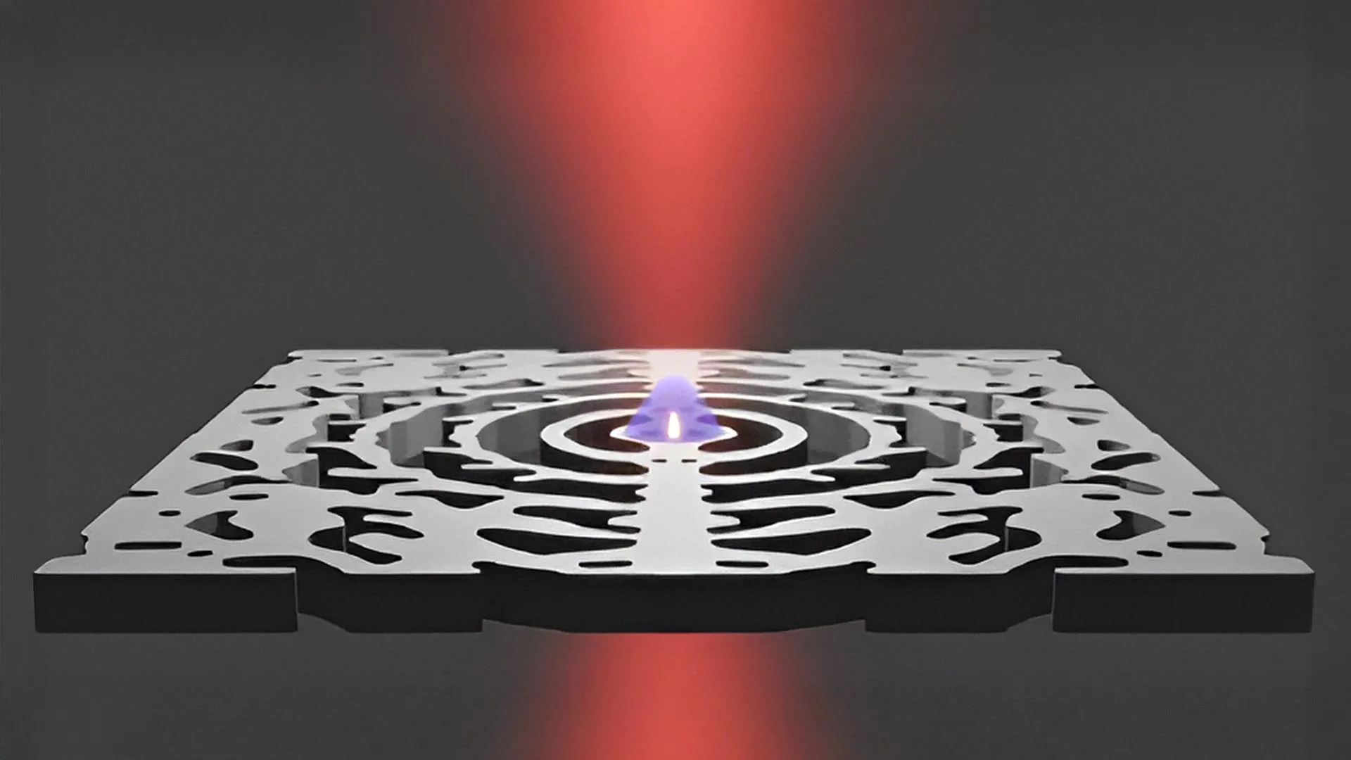
COPENHAGEN — In a development that could fundamentally reshape the architecture of modern electronics, researchers at the Technical University of Denmark (DTU) have successfully engineered a groundbreaking nanolaser. This microscopic marvel of optical physics marks a critical, long-sought milestone toward a paradigm shift in computing: replacing the electrical currents that have powered microchips for decades with pure beams of light.
Published in the peer-reviewed scientific journal Science Advances, the discovery details a hyper-compact laser capable of functioning at room temperature while confining light to an unprecedentedly small physical footprint. If successfully scaled and integrated into commercial manufacturing pipelines, this technology could pave the way for a new generation of computers, smartphones, and massive data centers that operate at blazing speeds while slashing energy consumption by up to 50 percent.
Main Facts
The core innovation centers on the ability to trap and concentrate light within an exceptionally tiny space known as a nanocavity, pushing past traditional boundaries of how small a functional laser can be constructed.
- The Core Technology: Researchers at DTU Electro, in collaboration with design experts from DTU Construct, built a nanolaser that tightly couples photons and electrons within a microscopic region. When stimulated by an external light source, the device generates coherent laser light efficiently at room temperature.
- The Paradigm Shift: While global telecommunications and long-haul internet data already rely extensively on fiber-optic cables carrying light signals, individual computer processors remain dependent on copper wires and electrical resistance. Transitioning to intra-chip optical communication means data could travel across microprocessors at the speed of light with virtually zero thermal resistance.
- Massive Energy Savings: According to lead researchers, integrating thousands of these nanolasers onto a single silicon microchip could slash overall computing energy consumption by as much as 50 percent—a critical win for data centers grappling with soaring global electricity demands and carbon footprints.
- Multisector Impact: Beyond consumer electronics and high-performance computing, the extreme light concentration achieved by the nanolaser opens up transformative possibilities in healthcare, including high-resolution biomedical imaging and ultra-sensitive diagnostic sensors.
Chronology: The Road to the Nanolaser Breakthrough
The creation of the DTU nanolaser is the culmination of years of multidisciplinary research, drawing on advanced materials science, nanoscale engineering, and topological optimization.
Foundation and Conceptualization (Late 2010s)
For years, physicists and electrical engineers understood the theoretical advantages of silicon photonics—the use of light rather than electricity to route data inside computer chips. However, a major bottleneck persisted: conventional lasers were simply too bulky to be integrated onto microchips alongside billions of microscopic transistors. Shrinking a laser typically led to severe optical losses, rendering it inefficient or incapable of operating at room temperature.
The Nanocavity Design
A pivotal breakthrough came through an interdisciplinary collaboration at DTU. The light-trapping structure—the nanocavity at the heart of the new device—was originally conceptualized and developed by the research group of Professor Ole Sigmund at DTU Construct. Utilizing advanced computer-aided design and topological optimization algorithms, the team engineered a structure capable of confining light within a volume scaled to the wavelength of the light itself.
Fabrication in DTU Nanolab
Armed with this optimized optical architecture, researchers moved into DTU’s state-of-the-art clean room facility, DTU Nanolab. Here, precision nanofabrication techniques were deployed to construct the physical device. Fabricating structures at the nanoscale requires absolute environmental control, as a single speck of dust can ruin an entire batch of micro-optics.
Successful Demonstration and Publication
Following rigorous testing, the research team—led by Professor Jesper Mørk alongside Drs. Meng Xiong and Yi Yu from DTU Electro—successfully demonstrated that the device could concentrate both photons and electrons in the same microscopic region, achieving lasing action at room temperature with minimal energy overhead. The findings were formally accepted and published in Science Advances, drawing international attention from the semiconductor industry.
Supporting Data and Technical Specifications
To understand the magnitude of the DTU breakthrough, one must examine the physics of modern microprocessors and the physical limitations that engineers have battled for over a decade.
The Thermal Bottleneck of Electronics
For the past fifty years, computing power has scaled in accordance with Moore’s Law, packing billions of transistors onto fingernail-sized silicon chips. As these transistors switch on and off millions of times per second, they push electrical currents through microscopic copper interconnects. This resistance generates immense thermal energy.
- The Heat Wall: Modern processors frequently hit thermal thresholds, forcing manufacturers to cap clock speeds to prevent physical melting or degradation of the silicon.
- Latency and Resistance: Electrical signals degrade over long distances inside a chip due to capacitive and resistive losses. Moving data across a large processor die consumes significant electrical power and introduces latency.
The Optical Advantage
Light, by contrast, does not experience electrical resistance in the same manner. Photons can cross paths without interacting, and optical channels do not suffer from the same RC (resistance-capacitance) delays that plague copper wires.
- Bandwidth Multiplier: Optical communication allows for wavelength-division multiplexing—meaning multiple distinct data streams can travel down the exact same physical channel simultaneously using different colors of light, exponentially multiplying bandwidth.
- Energy Efficiency Metrics: Professor Jesper Mørk estimates that shifting from electrical interconnects to optical networks-on-chip could reduce the energy required for internal data movement by up to 50 percent. In data centers—where cooling and powering servers consume a staggering percentage of the world’s electricity—such a reduction translates directly to gigawatts of saved power and millions of tons of avoided carbon emissions.
Official Responses and Expert Perspectives
The scientific community has responded to the DTU publication with significant enthusiasm, viewing the nanolaser not just as an academic novelty, but as a crucial stepping stone toward commercial optical microchips.
"The nanolaser opens up the possibility of creating a new generation of components that combine high performance with minimal size," stated Professor Jesper Mørk, co-author of the study from DTU Electro. "This could be in information technology, for example, where ultra-small and energy-efficient lasers can reduce energy consumption in computers, or in the development of sensors for the healthcare sector, where the nanolaser’s extreme light concentration can deliver high-resolution images and ultrasensitive biosensors."
Highlighting the collaborative nature of the breakthrough, Mørk and his co-authors—including Drs. Meng Xiong and Yi Yu—emphasized that the integration of optical physics with advanced structural design was essential. By combining the theoretical nanocavity models developed by Professor Ole Sigmund’s team at DTU Construct with DTU Electro’s semiconductor expertise, the research group successfully crossed a chasm that has troubled photonics labs worldwide.
Industry analysts note that while tech giants such as Intel, IBM, and various specialized photonics startups have spent years developing silicon photonics, the lack of an ultra-compact, energy-efficient nanolaser that can operate stably at room temperature has remained the missing link. The DTU design directly targets this vulnerability.
Implications for Global Technology and Society
The successful development of the DTU nanolaser heralds transformative potential across multiple high-tech industries over the coming decade.
1. High-Performance Computing and Artificial Intelligence
The explosive growth of artificial intelligence and Large Language Models (LLMs) has placed unprecedented demands on global computing infrastructure. Training modern AI models requires moving petabytes of data back and forth between processors and memory banks at blinding speeds.
Traditional electrical interconnects are rapidly becoming the primary performance bottleneck in AI supercomputers. By introducing nanolaser-driven optical links directly onto AI accelerator chips, data throughput could increase by orders of magnitude while drastically lowering power consumption, enabling the training of even larger and more sophisticated neural networks.
2. Consumer Electronics: Smartphones and Laptops
For end-users, the integration of optical microchips could translate into mobile devices that offer vastly superior computational performance with significantly extended battery life. Furthermore, because optical interconnects generate far less heat than copper circuits, smartphones and laptops could maintain peak processing speeds for much longer periods without triggering thermal throttling or requiring noisy cooling fans.
3. Sustainable Data Centers
Data centers are among the fastest-growing consumers of electrical power globally, with cooling systems often accounting for nearly as much energy as the servers themselves. Halting the escalation of data center power demands is an urgent climate imperative. Nanolaser technology offers a direct pathway toward reducing the thermal output of server racks, allowing for denser, greener, and more efficient cloud computing infrastructure.
4. Revolutionizing Healthcare and Biosensing
Beyond computing, the extreme light-concentration capabilities of the DTU nanolaser hold profound promise for medical diagnostics. By compressing light fields into sub-micrometer spaces, the device can interact with biological molecules with extreme sensitivity. This could enable:
- Ultrasensitive Biosensors: Capable of detecting single disease biomarkers or trace pathogens in early-stage blood samples.
- High-Resolution Biomedical Imaging: Providing sharper, more detailed optical scans of cellular structures without invasive procedures.
The Path Forward: Challenges and Timeline
Despite the profound promise of the DTU nanolaser, researchers emphasize that significant engineering hurdles remain before the technology finds its way into consumer laptops or enterprise servers.
- Electrical Pumping: The current iteration of the nanolaser is optically pumped—meaning it requires an external laser beam to stimulate light emission. To be viable for commercial microchips, the device must be redesigned to operate via electrical pumping, running directly off standard microchip voltages.
- Manufacturing Scale: Transitioning from clean-room fabrication of prototype batches to high-volume semiconductor foundries (such as TSMC or Intel) will require rigorous standardization and compatibility with existing complementary metal-oxide-semiconductor (CMOS) manufacturing lines.
According to conservative estimates from the research team, overcoming these remaining technical challenges will require 5 to 10 years of sustained research and development.
Nevertheless, the DTU breakthrough has illuminated a clear, scientifically validated path forward. As the digital world strains against the physical limits of traditional electronics, light-based computing is no longer a distant science-fiction concept—and with innovations like the DTU nanolaser, it is moving steadily into reality.