









NEW DELHI — India’s long-anticipated entry into the global semiconductor fabrication arena is shifting from policy blueprints and groundbreakings to execution, engineering, and eventual economic reality. Over the next three to five years, the nation’s nascent chip ecosystem will transition through critical operational milestones—ranging from physical project commissioning and customer qualification to the notoriously difficult phase of yield stabilisation.
According to a comprehensive research report published by 360 ONE Capital, the true commercial payoff of India’s chip manufacturing push will require patience, structural depth, and intense focus on execution. While multi-billion-dollar fabrication plants (fabs) and outsourced semiconductor assembly and test (OSAT) facilities capture the headlines, the immediate economic engine will be powered by a wide array of ecosystem enablers, including industrial construction, specialised utilities, chemical supply chains, and engineering automation.
As the country looks ahead toward a projected domestic semiconductor consumption boom, analysts and industry stakeholders are closely monitoring whether India can successfully convert massive capital expenditures into commercially viable, globally competitive semiconductor output.
Main Facts
The transformation of India into a credible global semiconductor hub rests on a combination of surging domestic demand, targeted government fiscal backing, and the gradual building of a complete manufacturing supply chain.
At the core of the current landscape is the India Semiconductor Mission (ISM), an umbrella initiative designed to incentivize the establishment of semiconductor and display manufacturing ecosystems in the country. To date, 12 major projects have received official approval under the ISM framework, representing a cumulative capital investment exceeding $18 billion. Looking forward, a potential second iteration of the program—tentatively referred to as ISM 2.0—could catalyse upwards of $35 billion in additional investments, drawing global consortia, specialized materials suppliers, and advanced packaging firms to domestic shores.
The macroeconomic driver behind these investments is staggering domestic and regional demand. India’s semiconductor demand is projected to scale aggressively, climbing from approximately $56 billion in 2025 to more than $117 billion by 2030. This expansion implies a robust compound annual growth rate (CAGR) of roughly 16 percent, outstripping the growth rates of many legacy technology markets.
However, 360 ONE Capital’s research underscores a crucial caveat: manufacturing capacity is currently being built ahead of proven domestic demand and deep-tier supplier ecosystems. Consequently, the report emphasizes that execution will matter far more than corporate or governmental announcements.
Near-term financial opportunities will not immediately materialize in the balance sheets of pure-play chipmakers. Instead, value capture in the early years will concentrate among ecosystem enablers. These include providers of cleanroom infrastructure, ultra-pure water and specialized gas utilities, electronics manufacturing services (EMS), component suppliers, engineering firms, and automation and equipment support providers.
Direct fab and OSAT economics will take several years to mature, meaning investors must view the semiconductor theme through a 10-to-15-year horizon rather than treating it as a traditional, short-term earnings cycle.
Chronology of Development: The Roadmap to 2035
The evolution of India’s semiconductor ecosystem is charted across distinct, sequential phases over the next decade. Understanding this chronology is vital for policymakers, industrial planners, and institutional investors evaluating risk and reward.
Phase 1: Infrastructure and Ecosystem Enablers (Years 1–2 / Near-Term)
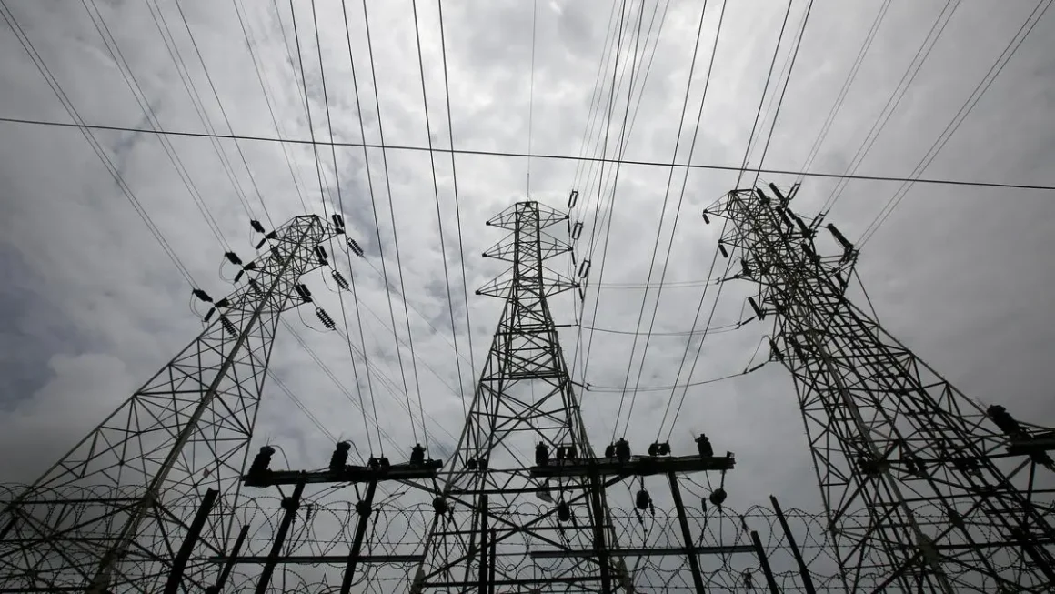
The opening act of India’s semiconductor story is defined by civil engineering, industrial construction, and utility provisioning. Building a semiconductor fab is vastly different from constructing a standard manufacturing plant; it requires ultra-clean environments, vibration-damped foundations, massive electrical substations, and uninterrupted supplies of ultrapure water and specialty gases.
- Key Activities: Groundbreakings, cleanroom construction, installation of heavy tooling, recruitment of specialized engineering talent, and the establishment of basic logistics and environmental safety protocols.
- Financial Beneficiaries: Engineering, Procurement, and Construction (EPC) firms, industrial automation specialists, equipment installation agencies, and suppliers of industrial gases and basic construction chemicals.
Phase 2: Commissioning, Process Qualification, and Pilot Runs (Years 2–4)
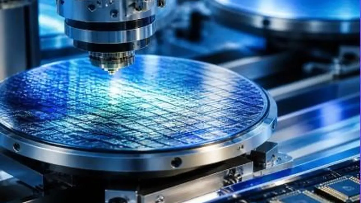
Once physical structures are erected and lithography, etch, and deposition tools are installed, the facilities enter the commissioning phase. This period is dedicated to calibrating complex machinery and running initial test wafers.
- Key Activities: Tool hook-up, baseline calibration, test-wafer runs, and initial process qualification. Facilities will test whether their internal environments can maintain the microscopic tolerances required for modern chip production.
- Financial Beneficiaries: Equipment vendors, maintenance and calibration service providers, and initial engineering support consultants.
Phase 3: Yield Stabilisation and Customer Qualification (Years 3–5)
This is universally acknowledged as the "valley of death" for new semiconductor operations. Moving from pilot production to commercial manufacturing requires stabilizing yields—the percentage of functional chips produced per silicon wafer.
- Key Activities: Iterative process adjustments to eliminate defect densities, optimization of cycle times, and rigorous third-party auditing. Simultaneously, chips must undergo customer qualification, where global fabless designers and OEMs test the locally manufactured silicon for reliability, thermal performance, and electrical tolerances.
- Financial Beneficiaries: Specialized testing and packaging houses, electronic design automation (EDA) software providers, and early-adopting domestic consumer electronics and automotive brands.
Phase 4: Localisation of Inputs and Advanced Packaging (Years 5–10+)
Once baseline production is stabilized and customer trust is secured, the ecosystem moves toward high-value integration. This includes the localisation of recurring raw materials—such as silicon wafers, photoresists, wet chemicals, and specialty gases—and the scaling of advanced packaging technologies like 2.5D/3D integration and Chiplets.
- Key Activities: Domestic sourcing of chemical inputs, establishment of regional R&D centers, and the expansion of OSAT capabilities to handle heterogeneous integration.
- Financial Beneficiaries: Specialty chemical manufacturers, domestic material science startups, advanced OSAT players, and long-term tech hardware manufacturers.
Supporting Data and Market Metrics
A quantitative breakdown of the metrics shaping India’s semiconductor trajectory illustrates both the scale of ambition and the magnitude of the capital commitment required:
- $56 Billion to $117 Billion: The projected expansion of India’s annual semiconductor consumption between 2025 and 2030, reflecting a ~16% CAGR.
- $18 Billion+: The total capital commitment represented by the initial 12 approved projects under the India Semiconductor Mission (ISM).
- $35 Billion+: The estimated additional investment that could be unlocked through the proposed ISM 2.0 ecosystem expansion.
- 10 to 15 Years: The strategic investment horizon recommended by financial analysts to properly evaluate the return on capital for foundational semiconductor manufacturing, as opposed to short-term cyclical earnings models.
- 7 Key Milestones: The operational checkpoints identified by market researchers—ranging from construction and process qualification to volume ramp-up and product mix diversification—that will dictate the success of individual ventures.
Official Responses and Industry Perspectives
The aggressive push to establish local semiconductor manufacturing has drawn commentary from across the industrial, financial, and governmental spectrum. Industry leaders emphasize that while the political will and financial incentives provided by New Delhi are historic, the laws of physics and global market dynamics will ultimately dictate success.
"The critical question is no longer whether factories can be constructed on Indian soil," notes the 360 ONE Capital report. "The critical question is whether they can achieve competitive yields, qualify with global customers, and operate at profitable scale."
Industry veterans point out that building a fab is only half the battle; maintaining high production yields in sub-micron manufacturing nodes requires an entrenched culture of zero-defect manufacturing, access to a deep pool of experienced process engineers, and seamless integration with global supply chains.
At the same time, policy advocates maintain that India’s vast and rapidly digitizing domestic market—spanning automotive electronics, telecommunications, consumer appliances, and defense systems—provides a built-in captive consumer base that few other emerging markets can match. By anchoring manufacturing locally, India aims to insulate its critical supply chains from geopolitical shocks, pandemics, and international logistics bottlenecks, ensuring long-term technological self-reliance.
Implications
The structural transformation currently underway across India’s industrial landscape carries profound implications for the domestic economy, the global technology supply chain, and the future of regional manufacturing.
1. Shift from Assembler to Creator
For decades, India’s electronics footprint was largely defined by final-stage assembly (often referred to as "SKD/CKD" assembly). The semiconductor mission fundamentally alters this paradigm, pushing the nation up the value chain into upstream component fabrication, silicon processing, and advanced packaging. If successful, India will transition from being merely a large consumer of imported technology to a foundational producer of the building blocks of the modern digital economy.
2. Workforce Upskilling and Educational Overhaul
The capital-intensive nature of semiconductor manufacturing requires an elite, highly specialized workforce. The next decade will witness a massive realignment in Indian higher education and technical training. Engineering curricula will need to place renewed emphasis on microelectronics, material science, chemical engineering, cleanroom protocols, and automated quality control. This demand for talent will likely drive higher wages and create an elite tier of specialized semiconductor engineers.
3. Supply Chain Localization and Regional Clusters
The growth of the semiconductor ecosystem is set to transform regional geography. States that successfully court fab and OSAT investments—such as Gujarat, Karnataka, Tamil Nadu, and Telangana—are emerging as high-tech industrial clusters. Over time, the need for just-in-time delivery of hazardous chemicals, high-purity gases, and precision spare parts will compel global chemical and equipment giants to set up manufacturing plants within India, reducing import dependency across the entire manufacturing value chain.
4. Strategic Autonomy and Economic Resilience
In an era marked by geopolitical volatility and trade fragmentation, domestic semiconductor capabilities are increasingly viewed as a pillar of national security. Securing a domestic source for automotive-grade chips, medical device processors, and defense electronics mitigates the risk of external embargoes and ensures that India’s broader manufacturing sector—including its burgeoning electric vehicle (EV) and 5G/6G telecommunications infrastructure—remains resilient against global supply chain disruptions.
Conclusion
India’s semiconductor journey is entering its most demanding and pivotal phase. As groundbreakings give way to the intricate realities of cleanroom commissioning, tool calibration, and yield optimization, the nation’s industrial sector faces a steep learning curve. While the ultimate economic returns will take a decade or more to fully materialize, the foundational steps taken today are set to redefine India’s position in the global high-technology hierarchy for generations to come.