










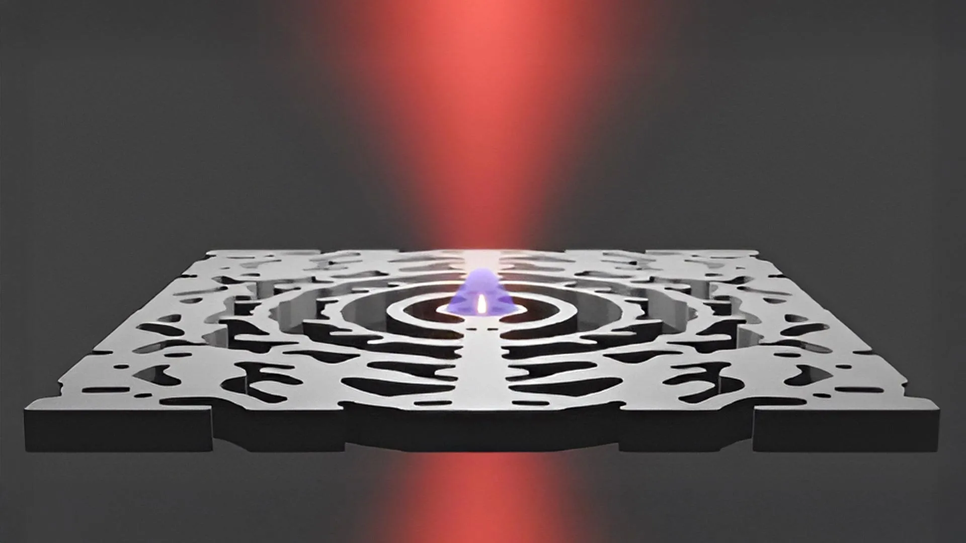
COPENHAGEN — In a breakthrough that could fundamentally rewrite the rules of modern computing, a team of researchers at the Technical University of Denmark (DTU) has successfully developed an ultra-compact nanolaser. Published in the prestigious scientific journal Science Advances, this milestone achievement brings humanity one step closer to a paradigm shift where microchips communicate not through traditional electrical resistance, but entirely via particles of light.
As the physical limits of conventional silicon-based microelectronics loom large, this innovation offers a tantalizing glimpse into a future where computers, smartphones, and massive global data centers operate at unprecedented speeds while slashing their energy consumption by up to half.
Main Facts: The Anatomy of a Breakthrough
At its core, the newly developed DTU nanolaser is an engineering marvel designed to overcome longstanding physical constraints that have baffled physicists for decades. Fabricated within the ultra-clean confines of the DTU Nanolab facility, the device achieves what was once considered virtually impossible: it compresses light into a nanocavity so intensely that it functions efficiently at room temperature while consuming negligible amounts of energy.
The primary highlights of the breakthrough include:
- The Optical Shift: By leveraging photons—the fundamental particles of light—instead of electrons, the nanolaser paves the way for microchips that transmit data at the speed of light internally.
- Radical Energy Efficiency: According to lead researchers, integrating these nanolasers into everyday computing architecture could reduce overall device energy consumption by as much as 50 percent.
- Overcoming the Size Limit: The device pushes past traditional boundaries regarding how small a functioning laser can be manufactured, utilizing a specialized nanocavity structure to trap and concentrate both photons and electrons within a microscopic region.
- Interdisciplinary Collaboration: The project represents a synthesis of advanced photonics and cutting-edge structural design, drawing on innovations originally pioneered by Professor Ole Sigmund’s research group at DTU Construct.
Chronology: The Road to the Nanolaser
The realization of this nanolaser did not happen overnight; it is the culmination of years of theoretical modeling, cross-disciplinary collaboration, and meticulous cleanroom fabrication.
Phase I: Theoretical Foundations and Light-Trapping (Years Prior)
The journey began with the fundamental challenge of light confinement. For light to be effectively utilized inside a microscopic laser, it must be trapped in a space smaller than its own wavelength. Years prior to the physical realization of the nanolaser, structural design played a pivotal role. The specialized light-trapping structure used in the device was originally conceptualized by Professor Ole Sigmund’s group at DTU Construct, who utilized advanced topology optimization to manipulate electromagnetic fields at microscopic scales.
Phase II: Fabrication and Cleanroom Realization (Recent Years)
Armed with advanced theoretical models, researchers shifted focus to the physical realization of the device. Working inside DTU Nanolab, the team—including key contributors Drs. Meng Xiong and Yi Yu from DTU Electro—began manufacturing structures designed to bridge the gap between theoretical nanophotonics and physical application.
Phase III: The Science Advances Publication (Present Day)
The culmination of these efforts arrived with the successful testing and documentation of the nanolaser. Operating at room temperature under optical excitation—where shining an external beam of light forces photons and electrons to concentrate in the same microscopic region—the device proved its viability. These findings were formally peer-reviewed and published in Science Advances, marking a definitive turning point for the field of silicon photonics.
Supporting Data: The Physics and Economics of Optical Computing
To understand why the DTU nanolaser is generating such intense excitement in the scientific community, one must examine the fundamental bottlenecks of contemporary computing architecture.
The Electronic Bottleneck
Much of the global internet already relies on light. Fiber-optic cables span oceans and continents, transporting staggering volumes of data across the globe using pulses of light. However, the moment that light reaches a local computer, router, or smartphone, it must be converted back into electrical signals.
Inside computers, data moves through microscopic copper and silicon electronic circuits. This traditional approach presents two massive, compounding problems:
- Heat Generation: Resistance in electrical circuits generates thermal energy. As microchips have grown denser—pushing Moore’s Law to its absolute physical limits—the heat generated by electrical resistance has become a primary barrier to increasing processing speeds.
- Transfer Limitations: Electrons move relatively slowly compared to photons, and moving them across complex circuit pathways creates latency and energy loss.
The Power of Photonic Integration
By bringing optical communication directly onto the microchip, nanolasers bypass these limitations entirely. Photons do not experience electrical resistance, meaning they generate virtually no heat during transit.
| Metric | Traditional Electronic Microchips | Proposed Nanolaser-Driven Optical Chips |
|---|---|---|
| Primary Carrier | Electrons (Electrical Signals) | Photons (Light Particles) |
| Energy Loss | High (due to electrical resistance) | Minimal (near-zero thermal loss) |
| Estimated Energy Savings | Baseline | Up to 50% reduction in computers |
| Operating Scale | Millimeter-to-nanometer electronic pathways | Thousands of integrated nanolasers per chip |
According to DTU Professor Jesper Mørk, integrating thousands of these microscopic lasers onto a single microchip will allow data to course through devices not as struggling electrical currents, but as coherent flashes of light. Mørk estimates that this transition could slash computer energy consumption by half, a monumental savings on a global scale.
Official Responses: Perspectives from the Research Team
The breakthrough has drawn praise from leaders within the academic community, who emphasize both the immediate scientific significance and the broad horizons the technology opens up.
"The nanolaser opens up the possibility of creating a new generation of components that combine high performance with minimal size," says DTU Professor Jesper Mørk, reflecting on the versatility of the new device. Mørk co-authored the landmark study alongside Drs. Meng Xiong and Yi Yu, forming a cohesive team from DTU Electro that bridged theoretical physics with practical engineering.
Mørk emphasizes that the applications extend far beyond consumer electronics:
"This could be in information technology, for example, where ultra-small and energy-efficient lasers can reduce energy consumption in computers, or in the development of sensors for the healthcare sector, where the nanolaser’s extreme light concentration can deliver high-resolution images and ultrasensitive biosensors."
The collaborative nature of the project has also been a point of institutional pride. By merging the optical expertise of DTU Electro with the advanced structural optimization techniques developed by Professor Ole Sigmund’s group at DTU Construct, the research team demonstrated the power of cross-disciplinary academic synergy.
Implications: A Glimpse into the Next Decade
While the realization of the nanolaser is a major triumph, researchers stress that it represents an early step toward a fully realized optical computing ecosystem. The scientific community has already identified the next critical hurdle that must be cleared before these devices can be commercialized.
The Road Ahead: Electrical Driving
Currently, the DTU nanolaser is activated by shining an external beam of light onto the device. The next major technical challenge for the research team is to make the nanolaser operate directly using electrical power.
Successfully integrating electrical contacts onto a nanolaser of this scale—without disrupting the delicate nanocavity trapping mechanisms—is a formidable engineering task. However, if researchers can achieve electrically driven nanolasers, the floodgates will open for commercial adoption.
Transforming Industries
The societal and economic implications of widespread nanolaser integration span multiple critical sectors:
- Consumer Electronics: Laptops, tablets, and smartphones could experience exponential leaps in processing power while running cooler and enjoying significantly extended battery life.
- Data Centers and Artificial Intelligence: Modern data centers—the sprawling server farms that power cloud computing and resource-heavy artificial intelligence models—consume vast quantities of electricity and require immense cooling infrastructure. Integrating optical microchips could drastically lower global data center power consumption, delivering profound climate benefits and easing strain on international electrical grids.
- Healthcare and Diagnostics: The nanolaser’s ability to concentrate light into an unimaginably small area translates to unprecedented precision in biomedical settings. This capability can be harnessed to build ultra-sensitive biosensors capable of detecting diseases at early molecular stages, as well as high-resolution imaging systems that reveal cellular structures with breathtaking clarity.
Timeline to Reality
How soon will consumers see this technology in the wild? Researchers estimate that the remaining technical challenges—chiefly the transition to electrical activation and large-scale manufacturing integration—can be successfully resolved within the next 5 to 10 years.
As laboratories worldwide race to refine silicon photonics, DTU’s latest contribution stands out as a defining milestone. By breaking past the traditional size limits of lasers and harnessing the power of trapped light, the team has illuminated a viable path toward a faster, cooler, and dramatically more sustainable technological future.